New diamond growth method slashes device temperatures by 41°F
Source: interestingengineering
Author: @IntEngineering
Published: 2/24/2026
To read the full content, please visit the original article.
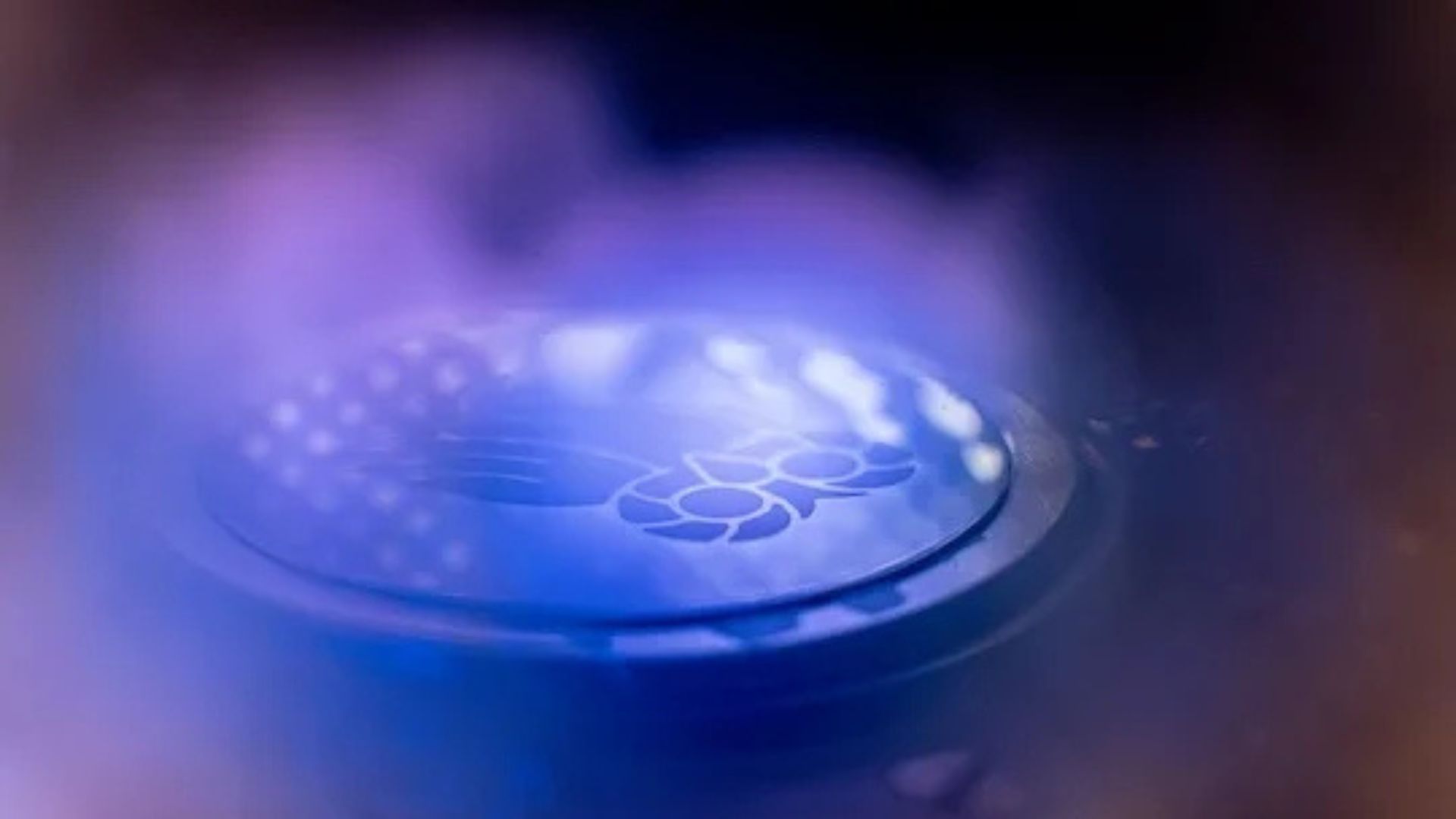
Read original articleResearchers at Rice University have developed a novel bottom-up method for growing patterned diamond surfaces directly onto electronic devices, significantly improving heat management by reducing operating temperatures by 23°C (41°F). This technique uses microwave plasma chemical vapor deposition combined with photolithography to create diamond layers precisely where needed, enabling better cooling for high-power technologies such as 5G, radar, and AI data centers. Unlike traditional top-down methods that are slow, expensive, and damaging, this approach grows diamond crystals from nanodiamond seeds on the device surface, offering a scalable and efficient solution.
The process has been successfully scaled to 2-inch wafers using two seeding techniques—photolithography for detailed patterns and laser-cut films for larger areas—making it suitable for mass production. It is compatible with various semiconductor base layers like silicon and gallium nitride, providing a versatile platform for integrating diamond thermal management across diverse electronics. The researchers emphasize that improved cooling with diamond can extend device lifespans, enhance performance,
Tags
materialsdiamond-growththermal-managementelectronics-coolingenergy-efficiencysemiconductor-manufacturingnanotechnology