World-first: Six layers stacked vertically to reinvent microchips
Source: interestingengineering
Author: @IntEngineering
Published: 10/18/2025
To read the full content, please visit the original article.
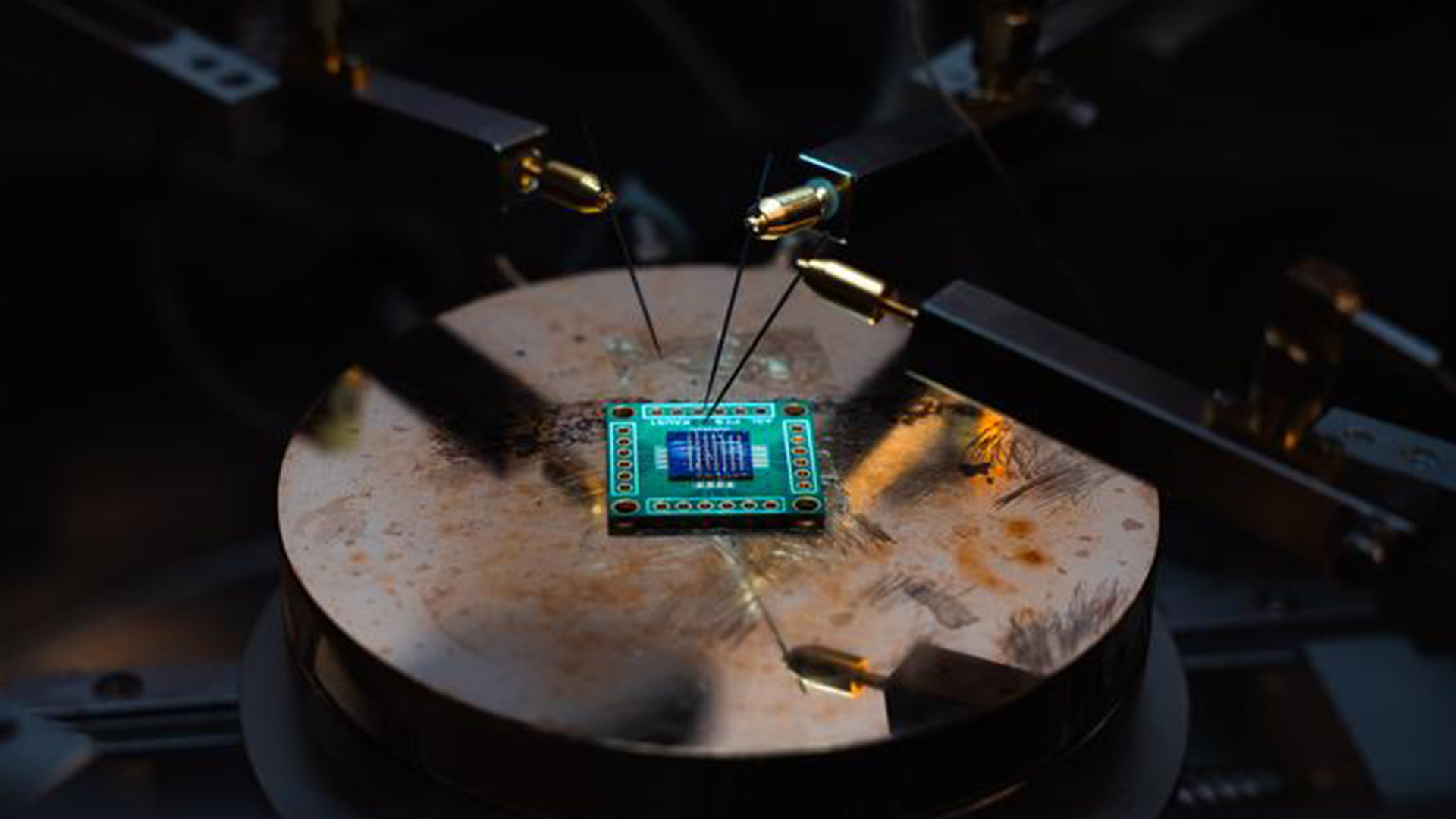
Read original articleScientists at King Abdullah University of Science and Technology (KAUST) have developed the world’s first six-layer hybrid CMOS microchip, significantly advancing beyond the previous two-layer limit in vertically stacked hybrid chips. This breakthrough enables much higher integration density by stacking circuits vertically rather than continuing to shrink transistor size, which is increasingly constrained by quantum effects and production costs. The team overcame key challenges such as heat damage to lower layers and precise layer alignment by innovating a low-temperature fabrication process that never exceeds 150°C, preserving the integrity of each layer. Their hybrid CMOS architecture combines inorganic and organic transistors, resulting in a stable, energy-efficient chip with six active layers—tripling the complexity of prior hybrid chips.
This novel vertical stacking approach opens new possibilities for ultra-thin, flexible, and efficient electronics, particularly benefiting wearable devices, medical sensors, and Internet of Things applications where compactness and low power consumption are critical. The technology also holds promise for space and environmental sensors due to its lightweight and high-performance
Tags
semiconductormicrochiphybrid-CMOSelectronicsmaterials-scienceenergy-efficient-technologyvertical-stacking